
Power mosfet smd 110v STC2326
Pobierz najnowszą cenę| Rodzaj płatności: | L/C,T/T,Paypal |
| Incoterm: | FOB,CFR,CIF |
| transport: | Ocean,Air |
| Porta: | SHANGHAI |

| Rodzaj płatności: | L/C,T/T,Paypal |
| Incoterm: | FOB,CFR,CIF |
| transport: | Ocean,Air |
| Porta: | SHANGHAI |
Model No: YZPST-STC2326
Marka: YZPST
B Triaki serii TA30
YZPST-STC2326
OPIS
STC2326 to tranzystor polowy z efektem polaryzacji N-Channel, który jest wytwarzany przy użyciu technologii wykopów DMOS o bardzo wysokiej gęstości komórek. STC2326 został zaprojektowany specjalnie w celu poprawy ogólnej wydajności przetwornic DC / DC z wykorzystaniem synchronicznych lub konwencjonalnych przełączników PWM. Został zoptymalizowany pod kątem niskiego poziomu bramki, niskiego poziomu RDS (ON) i dużej szybkości przełączania.
APLIKACJE
System zasilany
Konwerter DC / DC
Przełącznik obciążenia
CECHY
110V / 3A, RDS (ON) = 310mΩ przy VGS = 10V
Konstrukcja ogniwa o wysokiej gęstości dla wyjątkowo niskiego RDS (ON)
Wyjątkowa wytrzymałość i maksymalny prąd stały
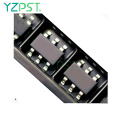
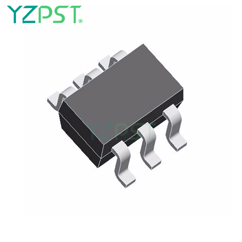
Projekt opakowania SOT-23-6L
KONFIGURACJA PIN (SOT-23-6L)
")
|
Pin |
Symbol |
Description |
|
1 |
D |
Drain |
|
2 |
D |
Drain |
|
3 |
G |
Gate |
|
4 |
S |
Source |
|
5 |
D |
Drain |
|
6 |
D |
Drain |
O RDER ING IN F O R M A T I O N
|
Part Number |
Package |
Part Marking |
|
SPN2326S26RGB |
SOT-23-6L |
26YW |
A B SOU L T E MA X I M U M R A T G G ( T A = 25 ℃ U n l s s o t h e r w i s e n o t e d )
|
Parameter |
Symbol |
Typical |
Unit |
|
|
Drain-Source Voltage |
VDSS |
110 |
V |
|
|
Gate –Source Voltage |
VGSS |
±20 |
V |
|
|
Continuous Drain Current(TJ=150℃) |
TA=25℃ |
ID |
3.0 |
A |
|
TA=70℃ |
2.0 |
|||
|
Pulsed Drain Current |
IDM |
10 |
A |
|
|
Power Dissipation |
TA=25℃ |
PD |
2.0 |
W |
|
TA=70℃ |
1.3 |
|||
|
Operating Junction Temperature |
TJ |
-55/150 |
℃ |
|
|
Storage Temperature Range |
TSTG |
-55/150 |
℃ |
|
|
Thermal Resistance-Junction to Ambient |
RθJA |
62.5 |
℃/W |
|
|
Parameter |
Symbol |
Conditions |
Min. |
Typ |
Max. |
Unit |
|
Static |
||||||
|
Drain-Source Breakdown Voltage |
V(BR)DSS |
VGS=0V,ID=250uA |
110 |
|
|
V |
|
Gate Threshold Voltage |
VGS(th) |
VDS=VGS,ID=250uA |
1 |
2.0 |
2.5 |
|
|
Gate Leakage Current |
IGSS |
VDS=0V,VGS=±20V |
|
|
±100 |
nA |
|
Zero Gate Voltage Drain Current |
IDSS |
VDS=80V,VGS=0V |
|
|
1 |
uA |
|
VDS=80V,VGS=0V TJ=125℃ |
|
|
5 |
|||
|
On-State Drain Current |
ID(on) |
VDS≥5V,VGS =10V |
3.0 |
|
|
A |
|
Drain-Source On-Resistance |
RDS(on) |
VGS= 10V,ID=3A |
|
0.26 |
0.31 |
Ω |
|
Forward Transconductance |
gfs |
VDS=10V,ID=3A |
|
2.4 |
|
S |
|
Diode Forward Voltage |
VSD |
IS=1A,VGS =0V |
|
|
1.2 |
V |
|
Dynamic |
||||||
|
Total Gate Charge |
Qg |
VDS=80V,VGS=10V ID= 5A |
|
9 |
13 |
nC |
|
Gate-Source Charge |
Qgs |
|
2 |
|
||
|
Gate-Drain Charge |
Qgd |
|
1.4 |
|
||
|
Input Capacitance |
Ciss |
VDS=25,VGS=0V f=1MHz |
|
508 |
|
pF |
|
Output Capacitance |
Coss |
|
29 |
|
||
|
Reverse Transfer Capacitance |
Crss |
|
16.5 |
|
||
|
Turn-On Time |
td(on) |
VDD=50V,RL=10Ω ID=3A,VGEN=10V RG=3.3Ω |
|
2 |
|
nS |
|
tr |
|
21.5 |
|
|||
|
Turn-Off Time |
td(off) |
|
11.2 |
|
||
|
tf |
|
18.8 |
|
|||
")
")


Tel: 86-514-87782298
Whatsapp: +8613805278321
Adres: 3rd Floor, Weiheng Building No.20 B Area, Yangzhou, Jiangsu China
Witryna internetowa: https://pl.yzpst.com


Privacy statement: Your privacy is very important to Us. Our company promises not to disclose your personal information to any external company with out your explicit permission.
Fill in more information so that we can get in touch with you faster
Privacy statement: Your privacy is very important to Us. Our company promises not to disclose your personal information to any external company with out your explicit permission.